三鑫新材料有限公司, 有限公司: 先进陶瓷领域的世界领先者 2008 年, 专业生产陶瓷研磨介质, 采矿业的耐磨零件和结构部件, 电子的, 制药, 航空航天和其他行业.
三鑫新材料有限公司, 有限公司: 先进陶瓷领域的世界领先者 2008 年, 专业生产陶瓷研磨介质, 采矿业的耐磨零件和结构部件, 电子的, 制药, 航空航天和其他行业.
我们随时准备回答任何问题并提供有关我们的碳化硅陶瓷产品的详细信息 (碳化硅), 以及综合工程和制造服务. 不管, 无论您是处于定制原型的开发阶段还是针对极端工业环境扩大批量生产, 我们的专家团队将帮助您充分利用这种高性能材料.
SiC陶瓷广泛应用于采矿业, 活力, 化学, 冶金和半导体行业, 需要高耐磨性的地方, 耐热性和化学惰性.
我们严格按照客户规格制造碳化硅组件. 所有关键参数均可配置:
SiC 的化学纯度和类型 (黑色的, 绿色的, 红细胞干细胞, SSC, CVD)
微观结构和相组成
尺寸公差和几何形状
精加工
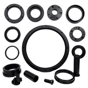
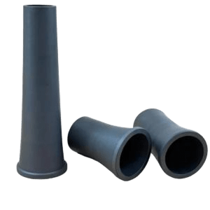
我们完成的项目包括:
高精度磨具产品
防火耐磨衬里
半导体用基板和晶圆
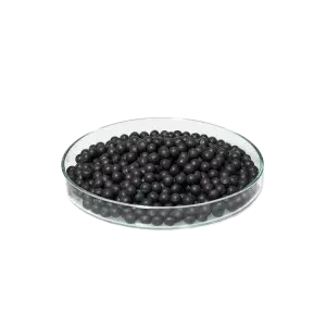
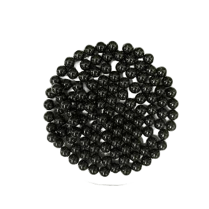
用于研磨矿石和水泥的碳化硅陶瓷球
准备开发定制 SiC 零件? 联系我们 - 我们的工程师使用 CAD 模型和快速原型技术, 这可以让您显着减少将产品推向市场所需的时间.
碳化硅 (碳化硅) 开业于 1893 美国化学家爱德华·古德里奇·艾奇逊. 在合成金刚石的实验过程中,他获得了材料, 后来被称为“金刚砂”, 这成为第一个人造磨料, 工业规模生产.
得益于其硬度 9,5 莫氏硬度, 碳化硅在20世纪初就已经取代了天然磨料。. 20世纪20年代开始积极用于耐火材料和工业炉衬。. 二战后,其半导体特性被发现, 包括宽带隙 (〜3.26电子伏特), 使 SiC 成为电力电子的关键材料.
自20世纪80年代以来,CVD技术的发展使得获得用于LED的超纯碳化硅成为可能, MOSFET 晶体管和高压器件. 如今,全球产量超过 1,5 百万吨/年, SiC市场估值超过 5 十亿美元, 电动汽车有什么贡献?, 可再生能源和5G网络.
碳化硅陶瓷是一种非氧化物共价材料,具有独特的机械性能组合。, 热性能和化学性能:
密度: 〜3.2克/立方厘米 (明显低于钢材)
硬度: 高压 ≈ 2100
弯曲强度: 到 400 兆帕
工作温度: 到 1600 ℃
导热系数: 90-490瓦/米·K
коэффициент теплового расширения: ~3,5 × 10⁻⁶ K⁻¹
SiC 抗氧化, 腐蚀, 热冲击和接触大多数酸和碱 (高频除外). 其自润滑微观结构确保低摩擦系数 (<0,2), 这使得该材料成为磨料和动态负载部件的理想选择.
尽管与氧化铝相比成本较高, SiC产品的使用寿命提高10-20倍, 从而降低总拥有成本 (总拥有成本) 经济效益高.
SiC 陶瓷有多种变体可供选择, 针对特定任务进行优化.
描述:
由石英砂和石油焦在艾奇逊窑炉中在 2200–2500 °C 的温度下生产. 碳化硅含量 - 97–99%, 存在铁杂质.
优点:
最佳价格/耐磨比
高断裂韧性
适合磨料磨具的批量生产
应用:
砂轮, 防火材料, 耐磨板, 以及用于采矿和水泥行业研磨机的 SiC 陶瓷球.
| 财产 | 单位. 改变. | 测试标准 | 黑碳化硅 | 绿色碳化硅 | 红细胞干细胞 | SSC | CVD碳化硅 |
| 材料 | – | – | 黑色的 | 绿色的 | 多孔的 | 稠密 | 电影 |
| 密度 | 克/立方厘米 | 国际标准化组织 18754 | 3,15 | 3,20 | 2,7 | 3,10 | 3,21 |
| 弯曲强度 | 兆帕 | ASTM C1161 | 400 | 450 | 250 | 400 | 500 |
| 抗压强度 | 兆帕 | 国标/T 8489 | 2000 | 2200 | 1500 | 2000 | 2500 |
| 杨氏模量 | GPa | ASTM C1198 | 430 | 450 | 300 | 410 | 460 |
| 断裂韧性 | 兆帕·米1/2 | ASTM C1421 | 4 | 4,5 | 3 | 4 | 5 |
| 泊松比 | – | ASTM C1421 | 0,16 | 0,16 | 0,17 | 0,16 | 0,15 |
| 硬度 HRA | 人力资源管理局 | 洛氏60N | 94 | 95 | 92 | 94 | 96 |
| 维氏硬度 | 高压V1 | ASTM C1327 | 2100 | 2200 | 1800 | 2100 | 2500 |
| 热膨胀 | 10⁻⁶ K⁻1 | ASTM E1461 | 3,5 | 3,4 | 3,6 | 3,5 | 3,3 |
| 导热系数 | 瓦/米·K | ASTM E1461 | 90 | 120 | 50 | 90 | 490 |
| 抗热震性 | ΔT (℃) | – | 600 | 650 | 500 | 600 | 700 |
| 最大限度. 步伐. (氧化) | ℃ | 无负载 | 1350 | 1400 | 1200 | 1350 | 1600 |
| 最大限度. 步伐. (恢复/惰性) | ℃ | 无负载 | 1350 | 1400 | 1400 | 1600 | 2000 |
| 体积电阻 (20℃) | 欧姆·厘米 | – | 10⁵ | 10⁴ | 10⁶ | 10⁵ | 10立方 |
| 介电强度 | 千伏/毫米 | – | 0 | 0 | 5 | 0 | 0 |
| 介电常数 (1 兆赫兹) | – | ASTM D2149 | 不适用 | 不适用 | 10 | 不适用 | 不适用 |
| 介电损耗 (20℃, 1 兆赫兹) | 正切δ | ASTM D2149 | 不适用 | 不适用 | 10⁻² | 不适用 | 不适用 |
笔记: 烧结等级的值; CVD 超过 (电导率 490 瓦/米·K, 纯度 99,9995%).
精密工程基准测试
SiC 具有优异的导电性/硬度, 优于半导体/热中的氧化物. 与金属/陶瓷的扩展比较:
| 特征 | 碳化硅陶瓷 | 氧化铝陶瓷 | 钢合金 | 碳化钨 |
| 强度和韧性 | 高的 (K_IC 4) | 抗压性强, 脆弱的 | 延展性, 容易疲劳 | 高的, 脆弱的 |
| 热稳定性 | 出色的 (1600℃) | 出色的 (1800℃) | 好的 (〜800°C) | 防火 (2800℃) |
| 耐磨性 | 卓越的 (高压 2100) | 最高等级 (高压 1500) | 缓和 (生锈) | 精英 (高压 2000) |
| 耐腐蚀 | 高惰性 | 出色的 (酸) | 倾斜 | 强的 (酸) |
| 透明度 | 不透明 (半透明CVD) | 半透明 | 不透明 | 不透明 |
| 生物相容性 | 高的 (国际标准化组织 10993) | 高的 | 各不相同 (有毒的) | 各不相同 |
| 电气绝缘 | 半导体 (10⁴–10⁵ 欧姆·厘米) | 出色的 | 导电 | 导电 |
| 磁性行为 | 无磁 | 无磁 | 铁磁 | 无磁 |
| 价格 (每公斤) | 缓和 ($20–50) | 低的 ($5–20) | 低的 ($1–5) | 高的 ($100+) |
| 密度 (克/立方厘米) | 3,2 | 3,9 | 7,8 | 15,6 |
SiC 属性提供生命周期优势:
SiC 在磨料/电子极端条件下大放异彩, 其硬度/导电性是不可替代的. 以下是扩展后的前 10 名:
SiC特性的结合巩固了其在高科技领域的地位, 市场估值为 $10 十亿千 2030 年.
标准 SiC 不透明黑/绿, 然而 CVD 和掺杂 (不适用) 选项可提供红外半透明效果.
SiC 部件通过粉末和蒸汽工艺形成,以提高密度 >99%. 下面是工作流程:
SiO2/碳混合物或 CVD 前体 (SiH₄/C₃H₈). 用于研磨球 - 粉末 <10 微米.
磨碎至 1–5 μm; 添加粘合剂和掺杂剂.
有机物去除温度高达 800°C.
2000–2200°C, 氩气; 血红蛋白/红细胞干细胞; 用于高密度的 HIP.
金刚石研磨至 Ra 0,01 微米; 球排序 >99% 球形度.
X射线, ASTM 弯曲, 三坐标测量机.
包装有证书, 每年可扩展至数百万种产品.
出口: 95%, 国际标准化组织 9001.
碳化硅轨迹: 更宽的带隙, 更环保.
盘子 200 电动汽车用毫米, 效率 +40%; 用于亚微米 PSR 的纳米 SiC 磨削.
3D 打印喷嘴/球, 浪费 -50%.
种植体用HA, 一体化 +20%.
量子位无缺陷.
碳化硅加工, 二氧化碳 -25%; 艾奇森生物炭.
复合年增长率 15% 到 $10 十亿千 2030 年, 电动汽车/可再生能源; 研磨介质 $2 十亿细分市场.